2D iSiPDR scanner for surface imaging of electrical parameters of low-resistivity semiconductors and thin films
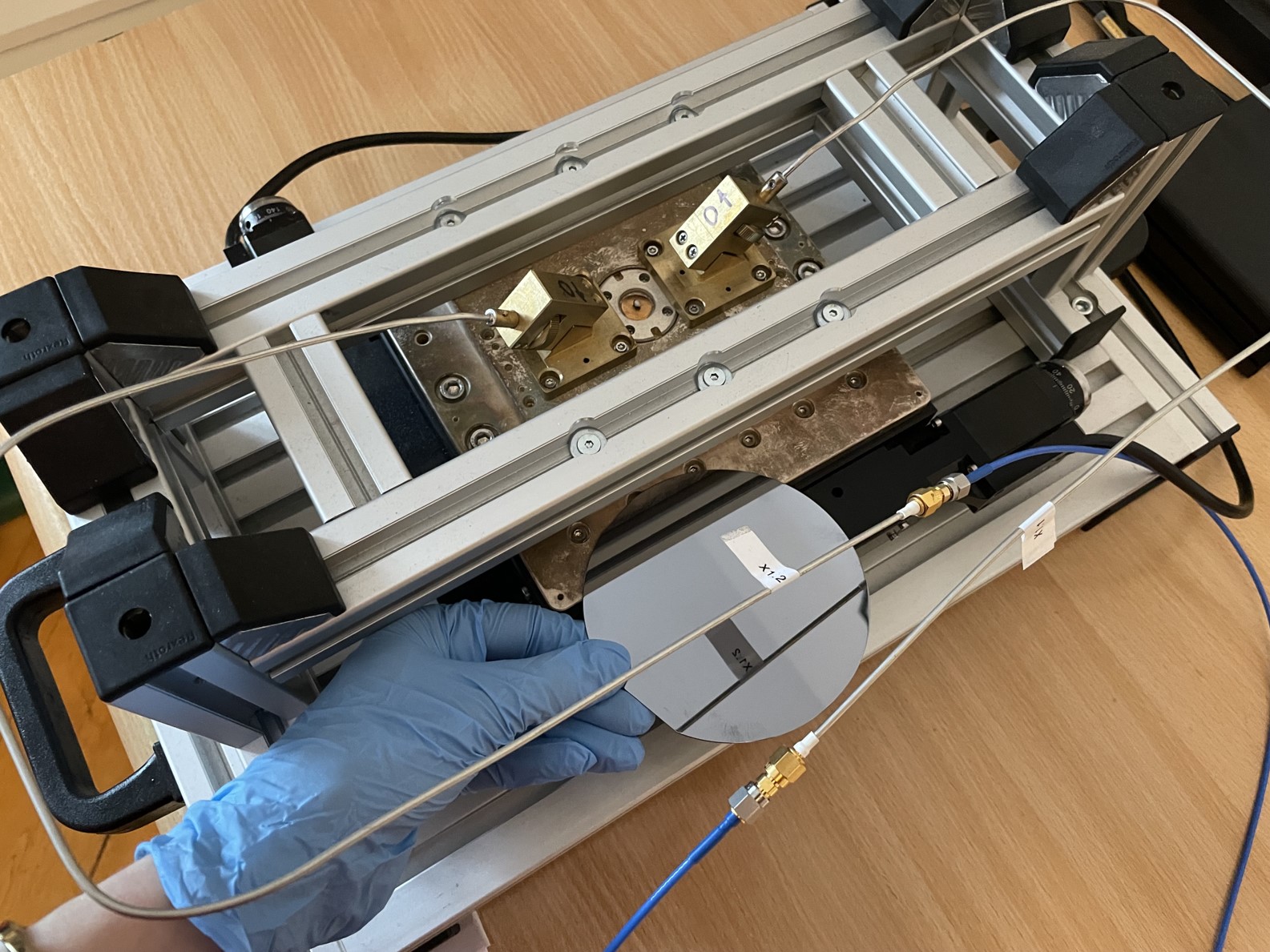
10 GHz iSiPDR scanner is based on single-post dielectric resonator method and is dedicated to low-resistivity semiconductors and thin films, delivering 2D maps of resistivity and surface resistance, respectively. It provides quantitative and qualitative measures of materials quality and uniformity. Next to its application to electronic materials like semiconductor wafers, it can be applied to conductive composite materials e.g. carbon-based polymer composites such as graphene-based anode materials for lithium-ion battery cells, volumetric composites for EMC applications, etc.
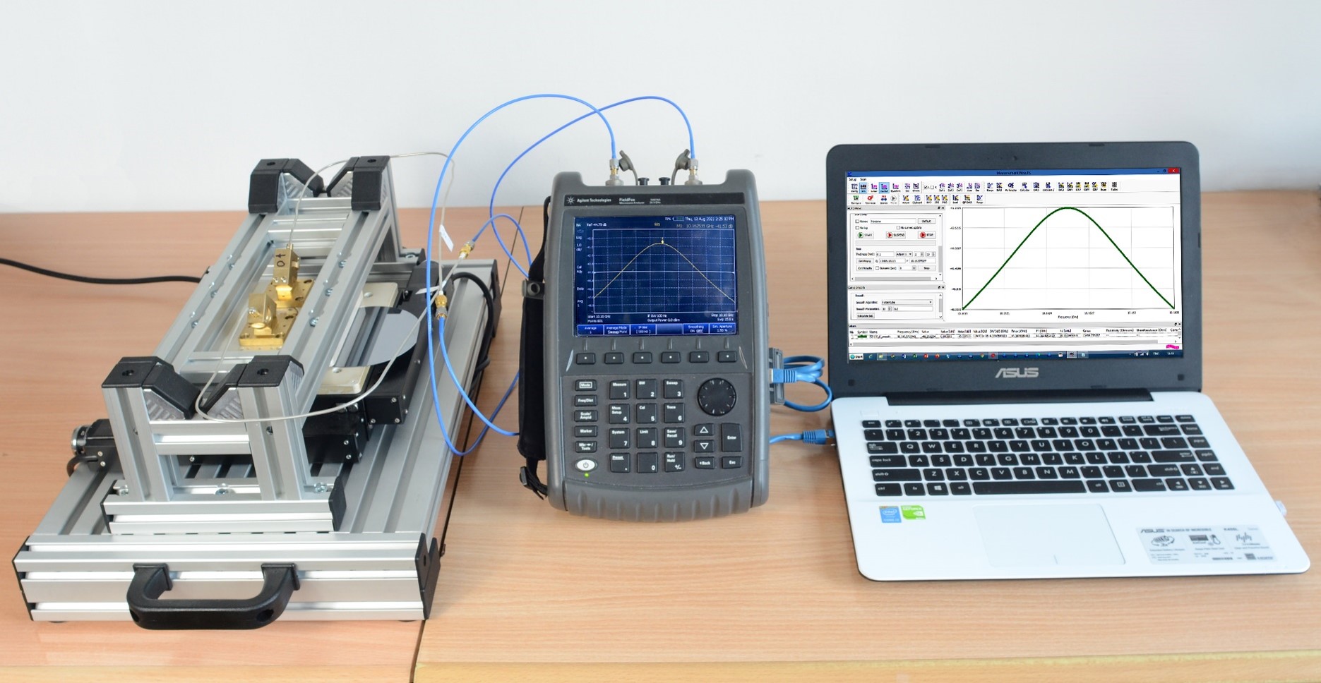
2D 10 GHz iSiPDR scanner with FieldFox VNA and scanner control app as developed within NanoBat project
The 2D iSiPDR scanner can be conveniently used with vector network analyzers...
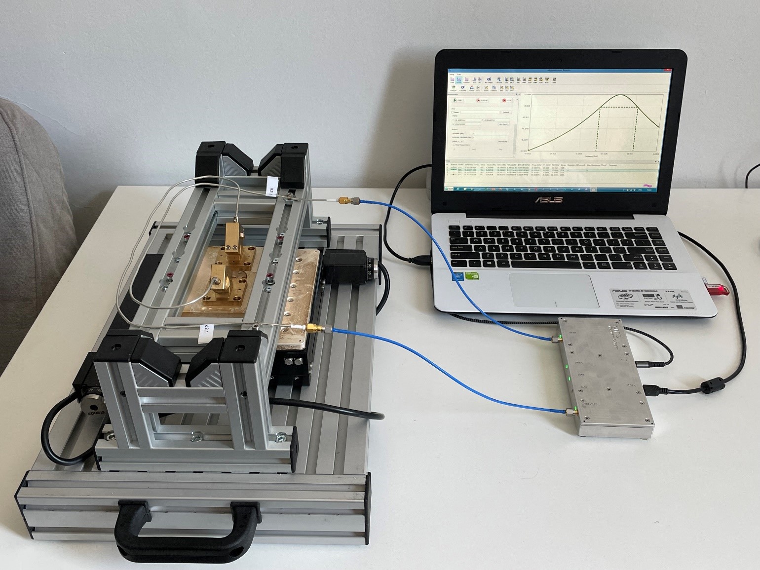
A portable and fully automated scanning setup: 2D 10 GHz iSiPDR scanner, Microwave Q-Meter, and scanner control app
... or QWED's portable, low-cost Microwave Q-Meter. Both measurement setups are supported by the Scanner Unit Control app making the characterisation procedure fully automated and conveniently steered from a laptop.
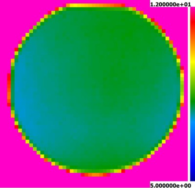
2D imaging of 4-inch silicon wafer of declared resistivity of 8 Ohm cm
The 2D iSiPDR scanner has been successfully applied in Horizon 2020 NanoBat project to 2D imaging and quantitative testing of carbon-based composites intended for anodes in lithium-ion batteries (see our paper).